Pic12f683 inverter circuit with project file version 1

PIC12F683 Inverter Circuit with Complete Project Files – Version 1

Welcome to an exciting project: the PIC12F683 Pure Sine Wave Inverter. This article provides everything you need to build your own efficient, cost-effective pure sine wave inverter. It includes detailed schematics, HEX code, project files, and even PCB designs for those interested in creating their own printed circuit boards (PCBs).

Introduction to the PIC12F683 Pure Sine Wave Inverter

This project focuses on creating a clean and stable 50 Hz sine wave output using the PIC12F683 microcontroller. The design is highly efficient and minimalistic, requiring only two integrated circuits (ICs), making it accessible for both beginners and experienced electronics enthusiasts.

The project is perfect for students looking for a simple yet impactful electronics project, particularly for final-year submissions. It combines cost-effectiveness, simplicity, and the satisfaction of building a functional and practical inverter circuit.


Why Choose the PIC12F683 Pure Sine Wave Inverter?

1. Simplicity and Flexibility

The circuit design is straightforward, involving just two 8-pin ICs, a few transistors, and MOSFETs. This makes it easy to assemble and troubleshoot, even for individuals with limited experience in electronics.

2. Ideal for Electronics Students

This inverter is an excellent choice for students or hobbyists who:

  • Need a reliable, budget-friendly project.
  • Want a practical circuit with real-world applications.
  • Seek an easy-to-understand design that facilitates learning.

3. Cost-Effective and Efficient

  • The design minimizes component requirements, reducing costs without compromising functionality.
  • By using readily available components, the project remains economical and accessible for anyone.

4. Open-Source and Customizable

All project files, including the schematic, HEX code, and PCB layout, are open-source. This allows users to modify and adapt the design to suit their specific needs.


Project Components and Resources

To build the PIC12F683 sine wave inverter, you’ll need the following:

Core Components

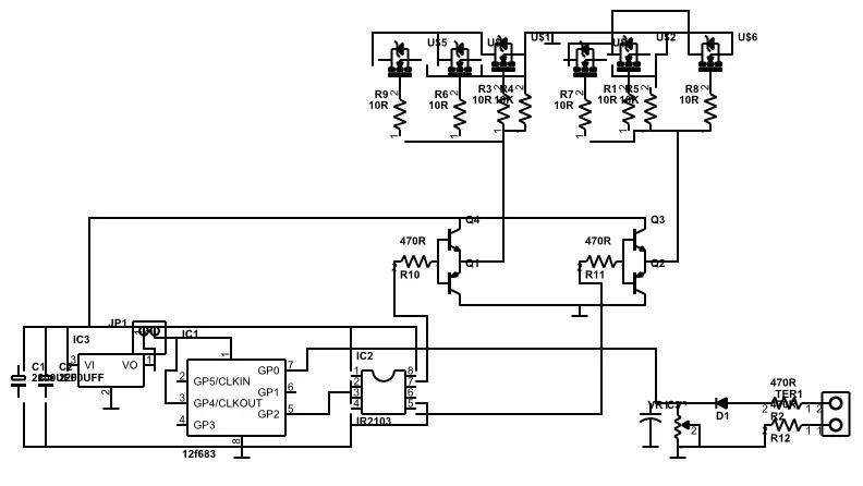
  • PIC12F683 Microcontroller: Acts as the brain of the inverter, generating the sine wave.
  • IR2103 MOSFET Driver: Ensures proper switching of the MOSFETs to generate high and low sides of the sine wave.
  • MOSFETs: Switch high-voltage DC to produce a sine wave output.
  • Passive components (resistors, capacitors, etc.) for the supporting circuitry.

Provided Resources

  • Schematic Diagram: A complete guide to assembling the circuit.
  • HEX Code: Precompiled firmware for the PIC12F683 microcontroller.
  • PCB Layout: For those who wish to create a professional-looking printed circuit board.
  • Demonstration Video: A visual guide to understanding the functionality of the inverter.
Challenges and Solutions

Issue with MOSFET Driver (IR2103):

The IR2103 MOSFET driver can encounter issues when connected to a 12V supply. The high-side output delivers 12V instead of the expected 6V. This occurs due to a 5-second delay in the microcontroller’s HEX file, causing the high side to turn on while the low side remains off. This can directly trigger the MOSFETs with voltage, potentially damaging the circuit.

Solution – Adding a Delay Timer Circuit:

To resolve this, a 5-second delay timer circuit is added. The timer output is connected to the VCC pins (1 and 8) of the IR2103, ensuring proper synchronization between the microcontroller and the MOSFET driver. This prevents premature activation of the MOSFETs and protects the circuit.


Step-by-Step Guide to Building the Inverter

1. Assemble the Circuit

Using the provided schematic, assemble the circuit on a breadboard or PCB. Ensure all connections are secure and components are placed correctly.

2. Program the PIC12F683

Upload the HEX file to the PIC12F683 microcontroller using a suitable programmer. Ensure the microcontroller is properly programmed and tested before integrating it into the circuit.

3. Add the Delay Timer Circuit

Integrate the 5-second delay timer circuit to address the MOSFET driver issue. Adjust the preset VR to achieve a delay of at least 5 seconds.

4. Test the Inverter

Before connecting a load, test the circuit to verify that it generates a clean sine wave at 50 Hz. Use an oscilloscope to confirm the waveform and ensure stable operation.

5. Integrate and Use

Once testing is complete, the inverter is ready for use. Connect a suitable load and observe the performance.


Advantages of This Inverter Compared to Others

  1. Low Cost: Ideal for students and hobbyists on a budget.
  2. Simplicity: minimal component count, with just two ICs and a few transistors.
  3. Customizable: Open-source project files allow users to modify and adapt the design.
  4. Educational Value: Perfect for learning and understanding the basics of sine wave generation and inverter design.

Downloads and Resources


Conclusion

The PIC12F683 Pure Sine Wave Inverter is a simple, efficient, and cost-effective solution for anyone interested in learning or building an inverter circuit. Whether you’re a student, hobbyist, or electronics enthusiast, this project offers a practical way to explore inverter design and sine wave generation.

Stay tuned for more updates and improvements by following this blog. Don’t forget to share your feedback and experiences with this project!

simple and small circuit | 12v
to 230v inverter

annotation-202022-04-08-20163430-1-2

I’m sharing an inverter project today that I think is the world’s most straightforward bi-stable inverter circuit.

Describe the idea of inverters that are bi-stable.

An inverter that uses a bi-directional flow of power to stabilize the output voltage and frequency is known as a bi-stable inverter. For applications requiring a steady output voltage and frequency, such as charging small electronic items like laptops, phones, and AC lamps, this kind of inverter is crucial.

the advantages of bi-stable inverter technology.

The application of bi-stable inverters has numerous advantages, such as:

They can lessen the wastage of energy.

They have the potential to reduce your electricity costs.

It can be utilized in the house in the event of a power loss.

They can assist you in lessening your reliance on the grid.

They can assist you in making less noise.

Anyone with little to no experience with electronics may complete this project because the circuitry is so basic.

Talk about the various kinds of bi-stable inverters.

The bi-stable inverter transistor: It employs two transistors, one of which turns on when the other turns off, and vice versa; this mechanism is known as a flip-flop.

IC Inverter with bi-stability: integrated circuit I’ll write a piece on integrated circuits that produce bi-stable inverters soon. Some examples of these circuits are IR2153 and CD4047.
A TRANSISTOR INVERTER IS THIS TYPE OF BI-STABLE INVERTER.
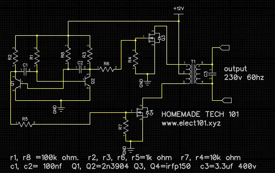
Its oscillator circuit, the Bi-Stable Multivibrator, consists of two transistors, eight resistors, three capacitors, two Mosfets, and a 12-volt transformer with a center cap (12v-0v-12v) Below is a list of the component values that were used.

components consist of:

4 pieces of 1k resistors

Two pieces of 10k resistor

Two pieces of 100k resistor

4.100nf (104j) two-piece capacitor

1 piece 3.3 uf (335 j) capacitor

Two BC3904 transistors

    Two pieces of IRFP150 MOSFET

    12v*2 transformer, also known as 12v-0v-12v transformer

    Below is a picture of the schematic for the inverter project.

    annotation-202022-04-08-20163430-1-2

    HERE IS THE VIDEO IN WHICH I TEST THIS PROJECT, AN INVERTER CIRCUIT.

    >> To get the schematic, click this link <<

    We appreciate you viewing our video and reading our article.

    Please tell your friends about this post.

    and remember to follow our YouTube channel.

    o

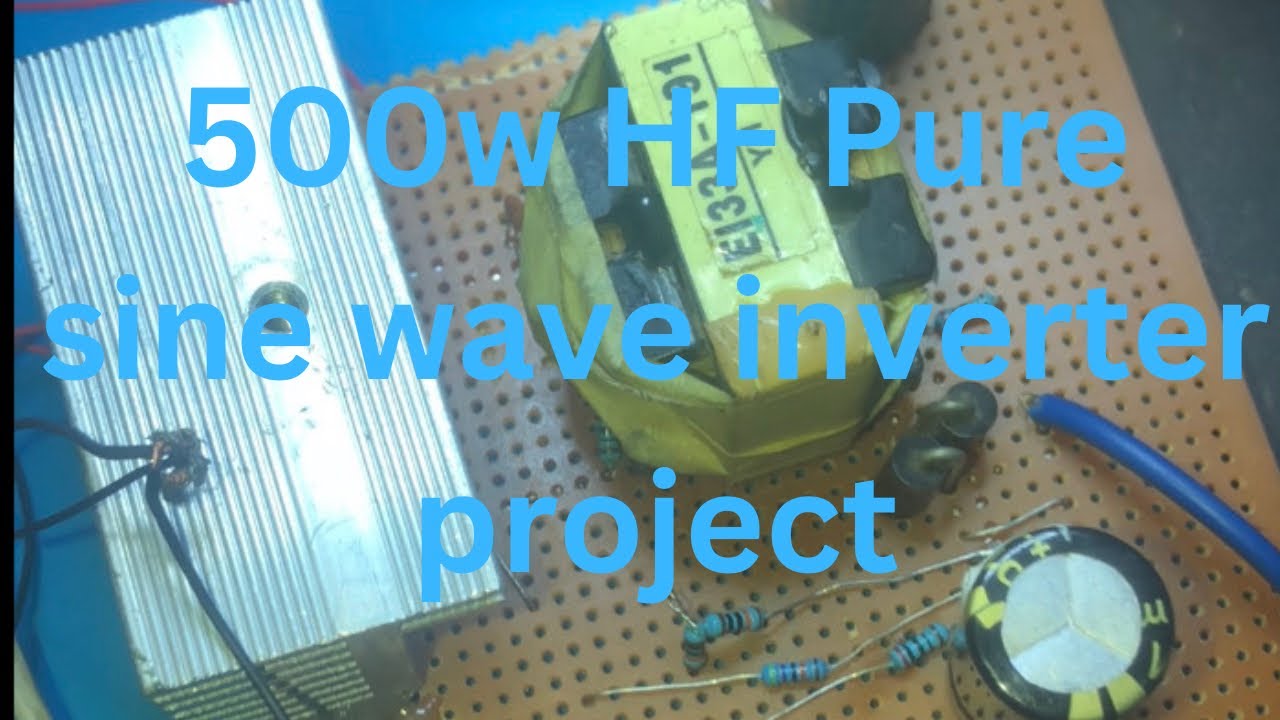
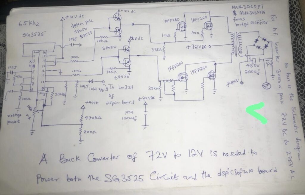
    12v to 310v dc HF inverter first stage circuit with SG3525 ic

    video-thumbnail-500w-hf-inverter-best-pure-sine-wave-inverter-project-part-1

    The SG3525 is a PWM regulator that can be used to control the output voltage and current of power. By adding a few extra components, it can be used to convert a 12V DC input to a 310V DC output.

    Here is a step-by-step guide on how to use the SG3525 to build a 12V to 310V DC power supply:

    Selecting the transformer: To convert the low-voltage input to a high-voltage output, you will need to choose a step-up transformer. One option is to select a transformer with a turns ratio of around 1:25. This implies that the secondary winding will have a significantly greater number of turns compared to the primary winding. For a 12V input, a suitable transformer would have a secondary voltage rating of approximately 300V.

    Make the necessary connections: Ensure that the SG3525 is properly connected to the input voltage, ground, and feedback pin. The feedback pin is used to control the output voltage. For this application, we will use voltage mode control with the SG3525, which can be designed to operate in either voltage mode or current-mode control.

    Connect the transformer: Connect the primary winding of the transformer to the output of the SG3525. The secondary winding should be connected to the diode and capacitor network.

    Include the diode and capacitor network: This network is used to rectify and filter the output voltage. A full-wave rectifier can be used with two diodes connected in a bridge configuration. To smooth the filtered output voltage, you can connect a capacitor in parallel with the output.

    Include the output load: Connect the load to the output of the power supply. Ensure that the load remains within the maximum current rating of the SG3525 and the transformer.

    Make adjustments to the SG3525 in order to achieve the desired output voltage. This task can be accomplished by making adjustments to the feedback voltage. This can be done by using a potentiometer or trimmer resistor that is connected to the output and feedback pins of the SG3525.

    There are a few important considerations to keep in mind when constructing a power supply using the SG3525:

    Component selection: Choose reliable components capable of handling the voltage and current ratings of the power supply. Using subpar components can result in the power supply becoming unstable and ultimately failing.

    Caution: High voltage DC poses a significant risk and can be potentially life-threatening. Ensure that the power supply is properly insulated and that necessary safety precautions are taken when dealing with the circuit.

    Improving productivity in the power supply can be achieved by selecting a transformer with a high turn ratio and reducing losses in the diode and capacitor network.

    To summarise, the SG3525 can be used to create a high-voltage DC power supply by regulating the output voltage and current. By carefully selecting components and prioritizing safety and efficiency, the SG3525 can become a valuable tool for powering a range of electronic devices.

    Simple push-pull inverter project with IR2153

    ir2153

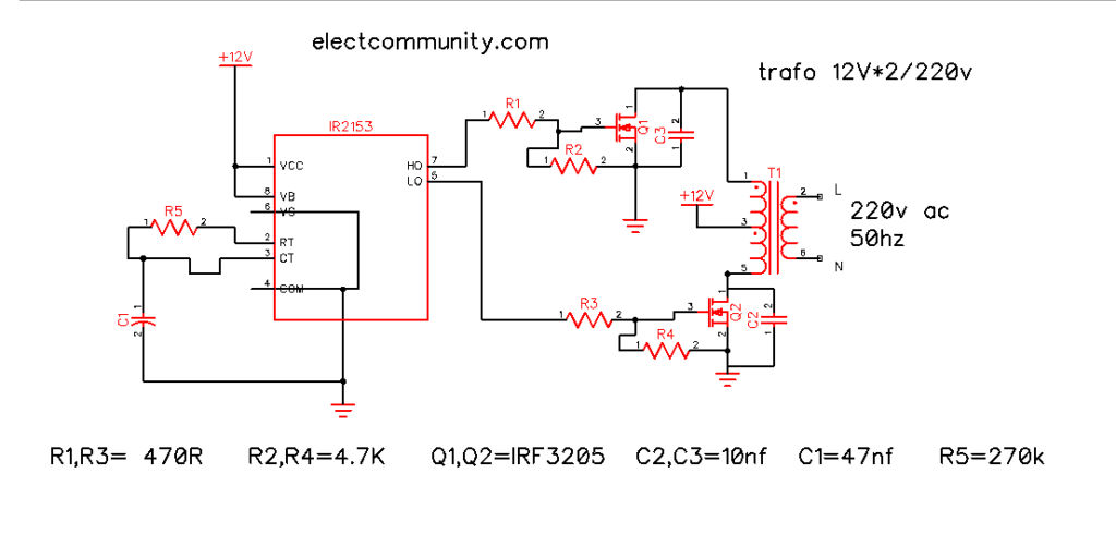
    This project that I am presenting today involves an IR2153 push-pull inverter. The circuit is designed to convert a 12VDC voltage from a battery into a 220V AC voltage. The circuit utilizes the IR2153 IC as the oscillator and MOSFETs to drive the transformer, resulting in a push-pull configuration that enables efficient voltage conversion. Here are the steps to construct an IR2153 push-pull inverter using MOSFETs.

    Components needed:

    – IR2153 integrated circuit

    – High-quality PCB BoaRequired components:

    The IR2153 integrated circuit

    – Utilizing MOSFETs IRF3205

    – Transformer (12V-0-12V to 220V)

    – Capacitors (47nF, 10nF)

    – Resistors (470Ω, 270kΩ, 4.7kkΩ)

    – Perf PCB Board

    Here are the steps:

    Begin by placing the components on the PCB board, starting with the IR2153 integrated circuit and MOSFETs.

    If you want to stabilize the circuit, you can connect a 2200uF capacitor to the positive DC source and the positive terminal of the transformer.

    Attach a 47nF capacitor to pin 3 and ground, and place a 10nF capacitor in parallel with the drain and source pins of each MOSFET.

    Attach the 270kΩ resistor to pins 2 and 3 of the IR2153 IC

    Attach the 470Ω resistor to the MOSFET gate driver.

    Connect one of the MOSFET’s drain pin to one side of the transformer and the second MOSFET’s drain to the other side of the transformer.

    Ensure that the sources of the MOSFETs are properly connected to the DC source.

    Lastly, attach the heat sink to the MOSFETs for effective heat dissipation.

    Test the inverter with a power load of up to 200 watts, just like an electrical engineer would do.

    In conclusion:

    A push-pull inverter utilizing MOSFETs, such as the IR2153, is an efficient and dependable option for converting DC voltage into high AC voltage. Ensure precise soldering of the MOSFETs, utilizing the appropriate component rating and adhering to their polarity. Exercise caution when handling the circuit, as it involves a high-voltage project.

    The push-pull configuration of the MOSFETs enhances the efficiency of the inverter, with two sides effectively managing the load. Using a heat sink to prevent the MOSFET from overheating is important. Follow the steps I demonstrated earlier to create the IR2153 push-pull inverter. To enhance power and efficiency, consider increasing the number of MOSFETs. Additionally, ensure that you select an appropriate transformer for your power requirements.

    Please consider following our social media page to stay updated at all times.

    Finally, connect the heat sink to the MOSFETs to ensure proper heat dissipation.

    dspic30f2010 inverter hex file inverter project full with hex file and schematic Giveaway

    dsp

    A sine wave inverter converts DC (Direct Current) power into AC (Alternating Current) power. It is commonly used in applications such as solar power systems, UPS (Uninterruptible Power Supply) systems, and portable power systems for camping or outdoor use.

    The DSPIC30F2010 microcontroller is widely recognized for its exceptional performance and affordability, making it a popular choice for implementing sine wave inverters. In this article, we will explore the design and implementation of a sine wave inverter using the DSPIC30F2010 microcontroller.

    Design Considerations:

    Before embarking on the design of the circuit and code for the sine wave inverter, it is important to take into account several design considerations. Here are some examples:

    The size of the components used in the circuit will be determined by the resulting power of the inverter. The power output can vary from a few watts to several kilowatts, depending on the specific application.

    The voltage output of the inverter will depend on the specific application. As an electrical engineer, you may encounter different voltage outputs in a solar power system, such as 120V AC or 240V AC.

    The outcome recurrence of the inverter will depend on the application. As an electrical engineer, it’s worth noting that the standard frequency in the US is 60Hz, whereas in Europe it’s 50Hz.

    Efficiency is a crucial factor to consider when evaluating the inverter’s impact on the overall performance and cost of the system. An inverter with improved efficiency will result in reduced power consumption and lower output intensity.

    The waveform of the resulting signal is an important consideration. A pure sine wave output is the preferred waveform as it produces minimal harmonic distortion and poses less risk of damaging delicate devices.

    Designing Circuits:

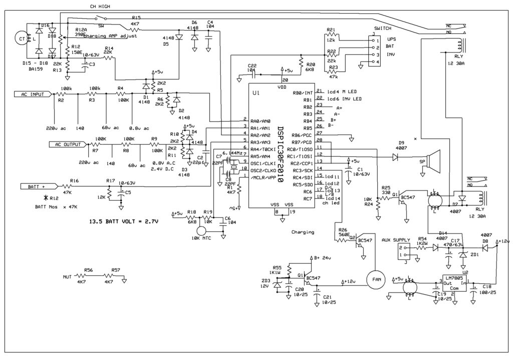
    The circuit design for the sine wave inverter using the DSPIC30F2010 microcontroller is shown in the figure below.

    Graph of a Sine Wave Inverter Circuit

    The circuit consists of several components:

    DC Power Supply: The DC power supply can be a battery or a solar board depending on the application.

    The DSPIC30F2010 microcontroller serves as the central component of the inverter. It generates a PWM signal that is used to power the MOSFETs.

    The IR2110 MOSFET driver is used to drive the MOSFETs. It produces a high voltage and high current output that is intended to power the MOSFETs.

    Utilizing MOSFETs, the DC power supply can be switched on and off at the frequency of the PWM signal. The circuit can use IRF3205 MOSFETs or similar options.

    LC Channel: The LC channel consists of an inductor and capacitor that work together to optimize the square wave output of the MOSFETs, resulting in a sine wave output.

    Load: The heap is linked to the outcome of the LC channel. The heap can serve as a resistive load or an AC motor depending on the application.

    Hey there, I’m hosting a giveaway for an awesome inverter project! This project is a digital pure sine wave inverter based on the dspic30f2010 microcontroller. It has some really cool functions that you’ll love!

    1. Presetting low battery levels through calibration
    2. Safeguarding against 440v mains

    3. The current range of the PWM battery charger is from 5A to 20A.

    1. Protection against inverter overload
    2. Protection against short circuits
    3. Sensitive to current and voltage in isolated AC mains.
    4. The voltage range is from 100V AC to 230V AC at 50/60 hertz, with low noise.

    LCD display is used to show various important information such as battery voltage, output voltage, input voltage, load wattage, charging current, and more. In this case, you have the option of choosing between a 7.162 or 164 LCD display.

    Video Of the inverter project info

    >>You can download the full project file here <<

    dspic30f2010 sine wave inverter source code

    dspic30f2010 inverter hex file

    please comment below.

    follow our youtube channel here to get notified when there is a new update.