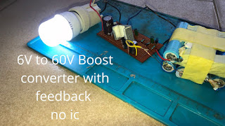
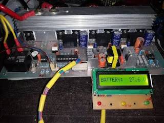
An easy DC-to-DC boost converter that can efficiently convert 6V to 100V

boost converter no ic

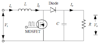
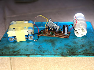
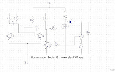
This project involves a basic boost converter that increases a 6V DC voltage to high-frequency AC. The AC is then converted using a full bridge rectifying diode setup with a capacitor at the output. What’s interesting about this project is that it doesn’t rely on any integrated circuits. Instead, the oscillator circuit is constructed using a two-transistor astable multivibrator circuit, with a frequency of 20kHz. Additionally, you have the flexibility to adjust the output voltage to your desired level, ranging from 5V to 100V DC, depending on your specific needs and application.

Here are the necessary components for this project:

MOSFET IRF3808.

All transistors are 2n2222a.

Using a PC817 optocoupler for feedback sensing

33k variable resistor

There are three capacitors with a capacitance of

102J, two capacitors with a voltage rating of

16V and capacitance of 470uF,

capacitor with a voltage rating of 400V and capacitance of 22uF

capacitor with a voltage rating of 50V and capacitance of 10uF.

Here are the diodes

bridge rectifier with a current rating of 2 amps

Zener diode with a voltage rating of 3.0 volts.

One LED indicator

Perf board for electronic prototyping

Transformer winding info

Primary turns: 4tns. Secondary turns: 60tns. Feedback wind turns 10 turns.

Here are the resistors you need:

100k 1pc

20k 2pcs

500R 2pcs

100R 1pc

1k 2pcs

Note:

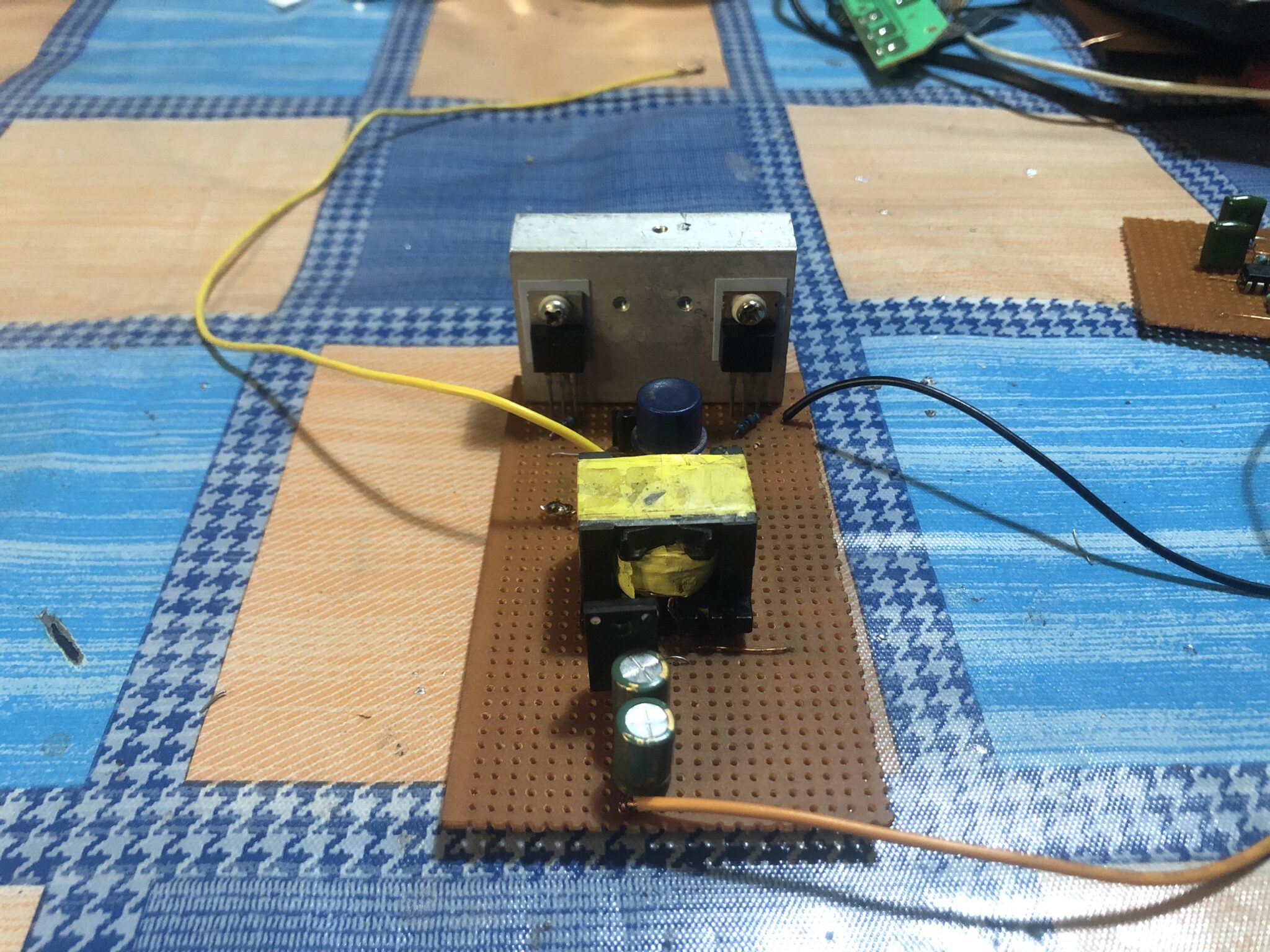
Using a thick heat sink is essential to ensure that the MOSFET does not overheat.
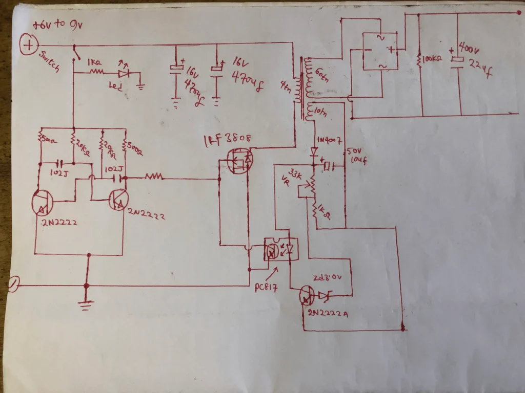
image-4

Key Factors to Keep in Mind:

To increase the efficiency of the circuit,

it is important to select appropriate component values, minimize losses in the inductor and diode, and ensure effective thermal protection for the MOSFET.

Switching converters

have the potential to generate electromagnetic interference (EMI) and radio frequency interference (RFI). For minimizing EMI/RFI, it is crucial to employ appropriate filtering components and layout techniques.

Note

It is important to note that switching converters have the potential to generate high voltages and currents, which can pose a safety risk. Ensure that proper safety measures are adhered to during the construction and testing of the circuit.

Conclusion

Building a DIY SMPS boost converter without an IC can be quite challenging, but with careful planning and assembly, it is definitely achievable. It is crucial to select suitable components, meticulously adhere to the schematic and assembly instructions, and conduct thorough testing of the circuit to guarantee dependable performance.
VIDEO HERE

>>>Click here to download the schematic capture<<<

A Simple Dc to Dc Cuk Converter Project Boost/Buck Functionality

Today I am reviewing my simple DC to DC Cuk converter project (low-side drive type of DC to DC buck-boost converter)

Firstly What is a Cuk converter

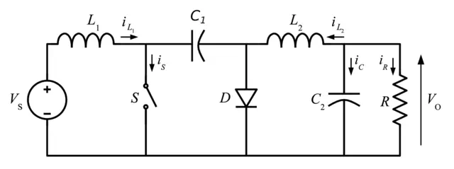
A Cuk converter is a type of converter that comprises both a buck converter and a boost converter which has only one switching device (Transistor, Mosfet, or IGBT), and the output current and energy are coupled with an electrolytic capacitor

These are the characteristics of a dc to dc cuk converter

  1. There is a reverse in the polarity of the output voltage side of the converter also similar to a buck-boost converter, in addition, to its polarity.
  2. It is a type of converter that has almost the same characteristics as the Buck-Boost Converter

Applications of Cuk Converter

  1. cuk converters are used as a voltage regulator
  2. They are used in hybrid solar-wind systems to make the output voltage constant

Advantages of Cuk Converter

  1. It has a low ripple current
  2. The efficiency is high up to 90%
  3. Switches(Mosfets, Transistor, or IGBT) are easy to drive because they are on a low-side drive
  4. Good EMI-EMI result which means the 2 inductors can share a core

Cuk Converter Topology Image below

Introducing my Simple Cuk Converter project.

Discuss the motivation for the project.

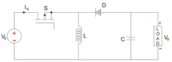
What motivated me to actually build a Cuk converter is that I have tried the normal buck-boost converter severally and I realized that their switch drive is very complex because the switching is a high side drive so I tried a Cuk converter out and it actually works.

Check this Buck-Boost image below to actually understand what I meant

Component list of the Cuk Converter Project

  1. Resistors
    • Variable resistor 20k ohms
    • resistor 470 ohms 4pcs
    • resistor 20k ohms 2pcs
    • resistor 2k ohms 1pc
    • resistor 3k ohms 1pc
  2. Transistors
    • Mosfet IRLB4132 1pcs
    • S8050 3pcs
  3. Diodes
    • 1n4007 1pc
    • 5A Schottky diode 1pc
    • Zener diode 3v 1pc
  4. Capacitors
    • 102 J capacitor 2pcs
    • 50v 10uf 1pc
    • 50v 1000uf 1pc
    • 35v 470uf
  5. Inductor
    • 2 ferrite E core wound with 0.2mm copper wire 20 turns each on core

Note the operating frequency of the circuit oscillator is 60khz

Here is the circuit diagram drawn below

Watch this video of me testing the project

Evaluate the results of the project.

With my testing and use of this project, my evaluation of my project is up to 85%

discussion of future directions for the Simple Cuk Converter.

I think in the meantime I will try to increase the workability and efficiency of this project the functionality of this project is it ok for use but I will just try to improve the project

>>>CLICK HERE TO DOWNLOAD THE PROJECT<<<

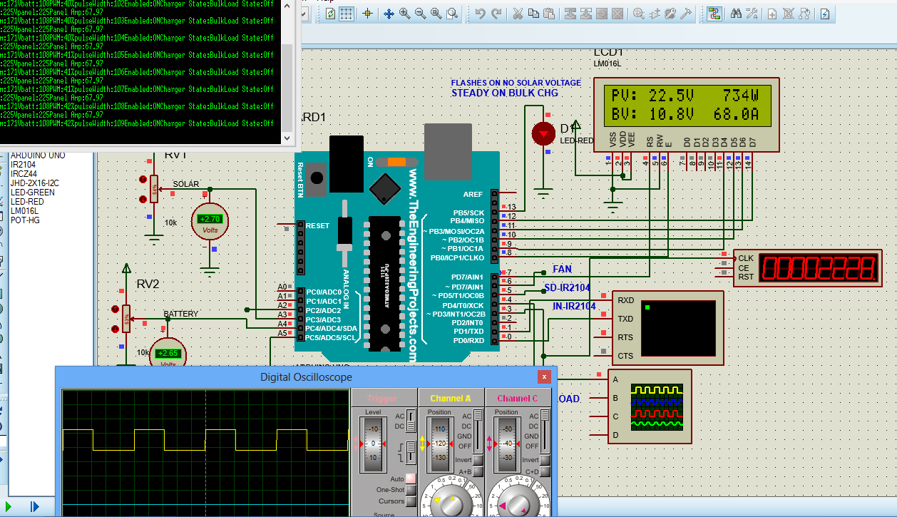
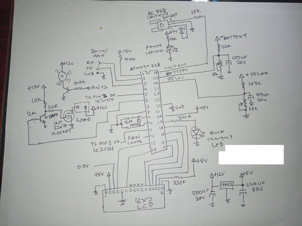
Atmege328 Mppt solar charge controller Project

atmega328

 Atmege328 Digital Mppt solar charge controller Project free download 

Although solar panels are expensive, solar chargers only convert only half of the solar electricity that hits them. Solar power converts approximately 99 percent when using MPPT chargers.

About the Mppt

Well, the foremost advanced star charge controller accessible within the market is most wall socket trailing (MPPT). The MPPT controller is a lot more refined and dearer. It has many benefits over the sooner charge controller. It is thirty to forty yet one more economical at cold. However, creating an MPPT charge controller is no bit advanced in comparison to a PWM charge controller. It needs some basic data on power physics. What Is MPPT? Most wall socket huntsman (MPPT) circuit is predicated around a synchronous buck device circuit… It steps the upper electrical device voltage right down to the charging voltage of the battery. The Arduino tries to maximize the watts input from the electrical device by dominating the duty cycle to keep the electrical device operational at its most wall socket. The Maximum wall socket huntsman (MPPT) controller increases charge current by operational the PV module in a manner that permits the module to supply all the abilities it’s capable of. A traditional charge controller merely connects the module to the battery once the battery is discharged. Once the 75W module during this example is connected to A battery charging at twelve volts power production is by artificial means restricted to regarding fifty-three watts. This wastes a humongous twenty-two watts or nearly half-hour of accessible power!

The MOSFET Driver: A MOSFET driver permits a coffee current digital signaling from a microcontroller to drive the gate of a MOSFET. A five V digital signal will switch a high voltage MOSFET exploitation of the motive force. A MOSFET incorporates a gate capacitance that you simply ought to charge so the MOSFET will activate and discharge it to modify off, a lot of currents you’ll offer to the gate the quicker you shift on/off the MOSFET, that’s why you utilize a driver.

atmega328

For this style, I’m employing an IR2104 [*fr1] Bridge driver. The IC takes the incoming PWM signal from the small controller, and so drives 2 outputs for a High and a coffee facet MOSFET. Input: First, we’ve to produce power for the gate driver. It is offered on Vcc (pin-1), and its worth is between 10-20V as per the information sheet. The high-frequency PWM signal from atmega ic goes to IN (pin-2). The finish-off management signal from the atmega ic is connected to SD ( pin 3).

main-control-1

Output: The 2 output PWM signals area unit generated from HI and LO pin. This offers the user the chance to fine-tune the dead-band shift of the MOSFETs. Charge Pump Circuit: The electrical condenser connected between VB and VS together with the diode kind of the charge pump. This circuit doubles the input voltage that the high switch may be driven on. but this bootstrap circuit solely works once the MOSFETs area unit shift

>>>Click here to download the Project for free<<<

powerful DC-to-DC boost converter with feedback, all without the use of an integrated circuit.

What exactly does a DC-to-DC boost converter do and how does it operate?

A DC-to-DC boost converter is utilized to amplify the voltage of a DC power supply. This converter is commonly employed in situations where the voltage of the DC power supply falls short of the necessary voltage.

 What are the advantages of utilizing a DC-to-DC boost converter?

There are numerous advantages to utilizing a DC-to-DC boost converter. One significant advantage is their ability to provide power to high-power devices. This is because they can deliver a higher voltage than what is typically provided by a standard USB port. In addition, these converters are capable of powering devices that require a voltage higher than what is provided by a typical outlet

What are the disadvantages of using a boost converter?

One drawback of utilizing a DC to dc boost converter is its potential for high power consumption and generation of noise. Using a dc to dc boost converter can have several potential drawbacks. If the converter malfunctions, the device will be unable to provide the required voltage to power the system. In addition, when the converter is not configured correctly, it may generate voltages that are inconsistent or imprecise. Lastly, in the event of an overload, there is a risk of causing damage to the device being powered by the converter.

Exploring the applications of a DC to DC boost converter

A DC-to-DC boost converter is a device that utilizes electrical energy to increase the voltage of DC power.

This device is commonly utilized to provide power to various electronic devices, including cameras and computers.

3. The DC to DC-boost converter is commonly utilized in the field of medical devices, including heart pacemakers.

The DC-to-DC boost converter is a versatile and compact device that can be utilized in various environments.

5. The DC-to-DC boost converter is a dependable device that can be utilized to provide power to various devices in different environments.

My straightforward project on a DC-to-DC boost converter without using an integrated circuit.

Diagram

VIDEO OF ME TESTING THE CONVERTER PROJECT

CLICK HERE TO DOWNLOAD THE PROJECT 

Circuit for Boosting Voltage from 12V to 19V using SMPS, SG3525, and IRFZ44 MOSFETs

19vto12v

This project is a basic SMPS 12v to 19v boost converter circuit or project for charging laptops and other devices that require a higher voltage than 12v.

Switched Mode Power Supplies (SMPS)

Switched-Mode Power Supplies, also known as SMPS, play a crucial role in the field of electronics by efficiently delivering controlled power. In this blog post, we delve into the intricacies of creating a 12V to 19V boost converter using the SG3525 PWM controller and IRFZ44 MOSFETs. This design is centered around the SG3525, a PWM controller. It offers precise control to optimize power source performance.

SG3525 functions as a PWM controller.

Our boost converter relies on the functionality of the SG3525 PWM processor. This versatile IC enables the generation of precise PWM signals by utilizing an external feedback loop, allowing for highly accurate control of the output voltage. Due to its versatility, it is frequently selected for various power source configurations, particularly when increasing the voltage from 12V to 19V.

MOSFETs in Switching Applications

In order to achieve efficient power conversion, a push-pull arrangement is implemented using two IRFZ44 MOSFETs as the switching elements. These MOSFETs excel at handling high-frequency switching, resulting in reduced power loss and improved overall efficiency.

Managing the Schedule and Gate Access

To ensure optimal switching, it is crucial that the gate control of the IRFZ44 MOSFETs functions effectively. Using 6.8kΩ gate-to-source resistors simplifies the management of the switching between on and off states. These 47Ω resistors that connect the PWM input of the SG3525 to the MOSFET gates play a crucial role in fine-tuning the switching characteristics, resulting in improved performance of the converter.

Altering the pulse and rectification

The SG3525 PWM signal is isolated from the power circuit using a push-pull pulse transformer. This enhances safety and reliability. Following the transformer, a Schottky diode and a 25V 470µF capacitor collaborate to effectively refine and rectify the pulsed output. This produces a reliable 19V DC output that can safely power electronic devices.

Understanding the feedback loop and voltage control

Maintaining a consistent output voltage is crucial. A feedback loop is established in our 12V to 19V boost converter by connecting a 10kΩ resistor to the output and a 10kΩ potentiometer. Thanks to this loop, the SG3525 has the ability to dynamically change the PWM duty cycle based on the difference between the desired output voltage and the real output voltage.

With the 10kΩ potentiometer, you have the ability to adjust the input to the SG3525, allowing for precise control over the output voltage. When the output voltage deviates from the set value, the PWM signal is adjusted by the feedback loop. The 19V output remains stable and accurate.

Component Utilized

Resistors

The values of resistors R1, R2, and R4 are all 47 ohms.

The resistance value is 220 kilohms.

The values of R7 and R8 are 6.8Kohms.

The values of R5 and R9 are 10Kohms.

The value of resistor R6 is 10 kilohms.

Mosfets

What are the values of Q1 and Q2? They are IRFZ44.

Integrated circuits (ICs)

U1 is SG3525.

Capacitors

The total energy of C1, C2, and C7 is 104J.

The value of C3 is 102J.

The values of C4 are 25V and 470UF.

Transformer

For the pulse transformer, the primary winding has a center tap with 4*2 turns, while the secondary winding has 6 turns.

Control

A power switch is used to control the flow of electricity in a circuit, allowing you to easily turn it on and off.

Watch the video here

In conclusion

The SG3525 12V to 19V boost converter with IRFZ44 MOSFETs is a dependable and efficient method for providing power. The SG3525 PWM controller, IRFZ44 MOSFETs, pulse transformer, and feedback loop were selected for their ability to deliver exceptional performance, reliability, and stability.

This boost converter exemplifies the seamless integration of advanced PWM control, high-frequency switching, and effective feedback systems. The seamless integration of these components ensures optimal power conversion for a wide range of electronic devices.

>>>Click here to download the project file<<<

Dspic30f2010 MPPT Solar Controller project

mppt-solar-charge-controller


Solar energy is a highly sustainable source of energy available today. With the increasing affordability and efficiency of solar panels, they are gaining popularity for both residential and commercial use. To maximize the energy output of a solar panel, it is crucial to use a solar controller that can track the maximum power point (MPP) of the panel. An excellent choice for a solar controller project is the DSPIC30F2010 microcontroller. It is highly suitable for implementing an MPPT (Maximum Power Point Tracking) algorithm.

The DSPIC30F2010 is a powerful 16-bit microcontroller from Computer Chip Innovation that offers a wide range of features, including an integrated ADC, PWM outputs, and a high-performance CPU. These elements aim to make the best decision for performing an MPPT calculation for a solar controller project. With the coordinated ADC, you can measure the voltage and current of the solar panel, and then use the PWM results to adjust the duty cycle of a DC converter. With the elite presentation CPU, the MPPT calculation is handled in real-time, ensuring that the solar panel always operates at its highest power point.

When setting up an MPPT solar controller with the DSPIC30F2010, the first thing you need to do is select an appropriate DC converter. The DC converter is responsible for stepping down the high-voltage DC output of the solar panel to a lower voltage that can be used to power the load. The choice of the DC converter will depend on the voltage range and power rating of the solar panel. There are several common types of DC converters that can be used, such as buck-boost, SEPIC, and Cuk converters.

Next, we need to perform an MPPT calculation to track the maximum power point (MPP) of the solar panel. Several MPPT calculations are available, but the most common ones include Irritate and Notice (P&O), Steady Conductance, and Fragmentary Open Circuit Voltage. These calculations involve continuously adjusting the duty cycle of the DC converter to track the maximum power point (MPP) of the solar panel. The DSPIC30F2010 has the capability to perform continuous calculations.

Additionally, the DSPIC30F2010 can be used to implement a user interface for monitoring and controlling the solar controller. It should be possible by using an LCD display, buttons, or a sequential point of interaction such as UART or SPI. The UI can be used to display the current power output of the solar panel, the battery voltage, and other relevant information. The client can also utilize the connection point to adjust the MPPT calculation parameters, such as the step size and the assembly measures.

One advantage of using the DSPIC30F2010 for an MPPT solar controller project is its ability to handle various obstacles and perform real-time calculations. The microcontroller is capable of handling obstacles from the ADC, the PWM outputs, and the UI, all while performing the MPPT algorithm calculations. Ensuring that the solar panel operates at its peak power point, even in varying environmental conditions.

In summary, the DSPIC30F2010 is a highly suitable microcontroller for implementing an MPPT solar controller project. With its incorporated ADC, PWM results, and superior execution CPU, this device is an excellent choice for performing an MPPT calculation, controlling the DC converter, and providing a user interface for monitoring and controlling the solar controller. By utilizing its advanced handling capabilities, the DSPIC30F2010 ensures that the solar board operates at its peak power point, resulting in optimal energy output and efficiency.

Features of this Dspic30f2010 Mppt

1. Achieving a remarkable working efficiency of 90%

2. Input voltage can reach up to 250V PV voltage.

3. The charging current can reach up to 70A, providing a high level of power.

4. The MPPT controller effortlessly detects the batteries. It is compatible with a wide range of battery systems, including 12V, 24V, 36V, 48V, 72V, 96V, 120V, and 144V.

IGBT Driver circuits commonly utilize the TLP250 as an Isolator driver for IGBTs.


6. Implementing an IGBT protection circuit to safeguard the IGBTs in the event of a fault.

7. Over-current protection is an important aspect to consider.

8. Protection against surges in solar or PV systems

There are three stages of charging control.

10. It can replace alternative MPPT controller boards.

11. Protection against high temperatures;

12. Concerning PV voltage protection

13. Change topology that is interleaved

14. Programming the hex file into the dspic30f2010 does not require any programming skills.

Take note of the inductor values.

Either 68uh or 73uh will work. The AWG 0.8mm (or gauge 20) copper wire can handle up to 5 Amps, meaning that the more wires used, the higher the current in each of the inductors.

Download the file by clicking here

Check out our YouTube channel here