Today, we will explore the working and design of a boost DC-DC converter. Let’s dive in!
What is a Boost DC-DC Converter?
A boost converter is a type of DC-DC converter that steps up the input voltage to a higher output voltage. It’s commonly used in applications where a higher output voltage than the input voltage is required. The main components of a boost converter include:
- Input capacitor
- Inductor
- Active switch (e.g., MOSFET)
- Passive switch (e.g., diode)
- Output capacitor
Working Principle
The boost converter operates in two phases: when the active switch is on and when it is off.
Phase 1: Active Switch On
When the active switch (transistor) turns on, the inductor starts charging and stores electromagnetic energy. The current flows through the inductor, and it builds up a magnetic field.
Phase 2: Active Switch Off
When the switch turns off, the inductor releases the stored energy. The inductor induces a flyback voltage, adding to the input voltage and boosting the overall voltage. This combined voltage forward-biases the diode, allowing current to flow to the load and charge the output capacitor. This process repeats continuously, providing a constant output voltage.
Control Mechanism
A closed-loop feedback system is used to maintain a stable output voltage. This system controls the switching time of the MOSFET, ensuring the inductor is charged optimally to produce the desired output voltage.
Designing a Boost Converter
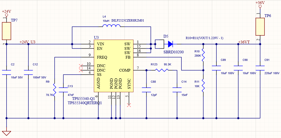
Instead of designing complex control logic from scratch, we can use an application-specific IC like the TPS55340 from Texas Instruments. This IC simplifies the design process and provides additional protections, such as under-voltage, over-current, over-voltage, and over-temperature protection.
Key Features of TPS55340
- Input voltage range: 2.9V to 32V
- Switching frequency: Up to 1.2MHz
- Internal MOSFET
- Output current: Up to 5A
- Excellent efficiency
Design Process
- Select Passive Components: Based on your design requirements (input voltage, output voltage, and output current), select appropriate passive components.
- Use TI Tools: Texas Instruments provides tools like an Excel sheet and the TI Webench for easy design and component selection. These tools help you input your design parameters and automatically calculate the required component values.
- Assemble the Circuit: Connect the components as per the design. The TPS55340 IC makes it straightforward to create a boost converter circuit with minimal effort.

Testing the Boost Converter
Once the circuit is assembled, testing it to ensure it meets the design specifications is crucial.
Test Setup
- Connect the DC power supply to the input.
- Connect an electronic load to the output.
- Use an oscilloscope to observe the switch node.
Test Results
- Input Voltage: 12V
- Output Voltage: 24V (constant)
- Load Regulation: The output voltage remains constant despite changes in load current.
- Line Regulation: The output voltage remains constant despite changes in input voltage.
Applications of Boost Converters
Boost converters are widely used in:
- Battery-operated devices
- Solar power systems
- LED drivers
These applications benefit from the ability to step up the voltage efficiently.
Conclusion
We hope this guide has helped you understand the working and design of a boost DC-DC converter. For detailed references and additional resources, check the description below. Don’t forget to hit the subscribe button for more informative videos!
Stay curious, stay innovative!